- English
- French
- German
- Portuguese
- Spanish
- Russian
- Japanese
- Korean
- Arabic
- Greek
- German
- Turkish
- Italian
- Danish
- Romanian
- Indonesian
- Czech
- Afrikaans
- Swedish
- Polish
- Basque
- Catalan
- Esperanto
- Hindi
- Lao
- Albanian
- Amharic
- Armenian
- Azerbaijani
- Belarusian
- Bengali
- Bosnian
- Bulgarian
- Cebuano
- Chichewa
- Corsican
- Croatian
- Dutch
- Estonian
- Filipino
- Finnish
- Frisian
- Galician
- Georgian
- Gujarati
- Haitian
- Hausa
- Hawaiian
- Hebrew
- Hmong
- Hungarian
- Icelandic
- Igbo
- Javanese
- Kannada
- Kazakh
- Khmer
- Kurdish
- Kyrgyz
- Latin
- Latvian
- Lithuanian
- Luxembou..
- Macedonian
- Malagasy
- Malay
- Malayalam
- Maltese
- Maori
- Marathi
- Mongolian
- Burmese
- Nepali
- Norwegian
- Pashto
- Persian
- Punjabi
- Serbian
- Sesotho
- Sinhala
- Slovak
- Slovenian
- Somali
- Samoan
- Scots Gaelic
- Shona
- Sindhi
- Sundanese
- Swahili
- Tajik
- Tamil
- Telugu
- Thai
- Ukrainian
- Urdu
- Uzbek
- Vietnamese
- Welsh
- Xhosa
- Yiddish
- Yoruba
- Zulu
What Is Sputtering Target?
2024-01-05 18:00:06
Today we focus on sputtering target materials which account for about 3% of the semiconductor material market.
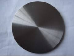
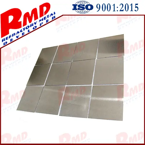
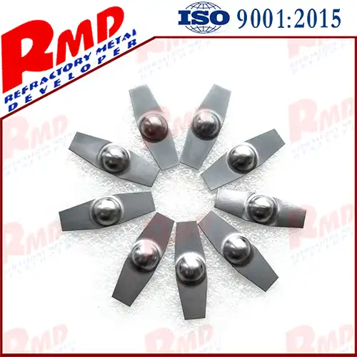
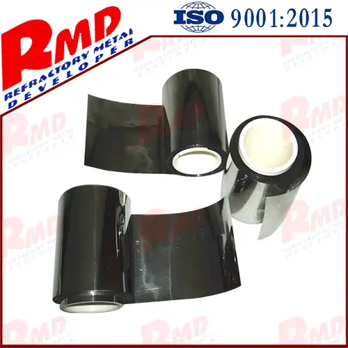
Simply put, the target material is the target material bombarded by high-speed charged particles. By replacing different targets (such as aluminum, copper, stainless steel, titanium and tantalum targets, etc.), different film systems (such as super-hard, wear-resistant and anticorrosive alloy films, etc.) can be obtained.
At present, the (high purity) sputtering targets can be divided into:
(1) metal targets (pure metal aluminum, titanium, copper, tantalum, etc.)
(2) alloy target (ni-cr alloy, ni-co alloy, etc.)
Ceramic compound target (oxide, silicide, carbide, sulfide, etc.).
According to the switch can be divided into: long target, square target, round target.
According to different application fields, it can be divided into: semiconductor chip target, plane display target, solar cell target, information storage target, tool modified target, electronic device target, other target.
Sputtering: that is, the process to be used repeatedly in the manufacturing of integrated circuits; Target material: it is an essential and important raw material in sputtering process.
The semiconductor interior is composed of tens of thousands of meters of metal wiring, and the sputtering target is a key consuming material for making these wiring. Like apple's A10 processor, a chip the size of a fingernail is covered with tens of thousands of meters of metal wires, which must be sputtered onto a high-purity metal target.
It is reported that apple's A10 chip is made of the high purity sputtering target material of kf electronics.
Sputtering target is a difficult material at the core of semiconductor wafer manufacturing. The chip has very high requirements on sputtering target, requiring high purity of target, generally above 5N (99.999%).
5N means there are five 9's, four N means there are four 9s or 99.99%, which one is more pure, you can see.
In the field of purification, every extra 9 after the decimal point increases the difficulty exponentially and the technical threshold is higher.
Application and market pattern
Now that we know the high purity sputtering target, and we know the aluminum, titanium, copper and tantalum of the metal target, how can we tell which metal should be used on a few inches wafer and which should be used in the advanced manufacturing process?
In semiconductor wafer manufacturing, the manufacturing process of 200mm (8 ") or less is usually dominated by aluminum, and the target materials are mainly aluminum and titanium. 300mm (12 ") wafer manufacturing, mostly using advanced copper interconnection technology, mainly using copper, tantalum targets.
At the same time, titanium is used as the main material of high dielectric constant metal grid technology, and aluminum as the main material of wafer bonding pad technology.
In general, with the increasingly wide use of chips, the number of chip market demand will increase, and the demand for aluminum, titanium, tantalum and copper, the four mainstream thin film metal materials in the industry, will certainly increase. At present, no alternative solutions can be found to replace these four thin film metal materials in terms of technology and economic scale, so there is no risk that these four materials will be replaced at present.
In terms of competition, due to the origin of sputtering coating process abroad, the required sputtering target products have high performance requirements. For a long time, the development and production of sputtering targets in the world are mainly concentrated in a few companies in the United States and Japan, with a high industrial concentration. Sputtering target manufacturers represented by honeywell (USA), Nippon mineral metals (Japan), and dongcao (Japan) occupy the majority of the global market share.
These enterprises in mastery of core technology of sputtering target materials production, the implementation of extremely strict security measures, restrictions on technology diffusion, continuous expansion of horizontal and vertical integration at the same time, to expand business tentacles actively to sputter deposition of various applications, firmly grasp the initiative sputtering target materials markets around the world, and leading the global sputtering target materials industry technology progress.
As for its application fields, they are mainly concentrated in semiconductor industry, flat panel display industry (including touch screen industry) and solar cell industry.
